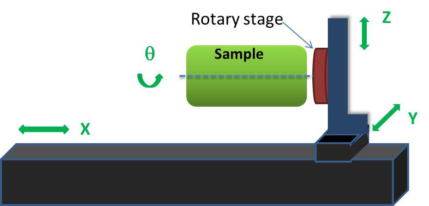
ARP announces terahertz nano-scanner for sub-surface inspection and 3D imaging
Main features
Fine scale inspection: a resolution of 25 nm
Layer by layer non-destructive inspection
Scanning area: up to 200 mm by 200 mm (can be tailored to other sizes)
Scanning speed: currently 10 mm/s (max) (can be increased per need)
Simultaneous reflection and transmission measurements
Reconstructive 3D imaging (no camera needed)
A paper for wafer inspection is here:
Effective testing for wafer reject minimization by terahertz analysis and sub-surface imaging
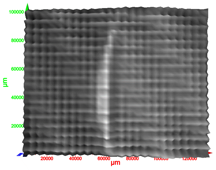
Surface plot of a patterned wafer reveals problem areas.
Layer-by-layer inspection is done for inspecting each layer individually. See
the video clip.
https://www.youtube.com/watch?v=Jpf_Ihq4HsI
Order
Click here for ordering information
Applied Research & Photonics, Inc.
470 Friendship Road, Suite 10
Harrisburg, PA 17111
e-mail: info@arphotonics.net
Phone: 717-220-1003
Fax: 717-566-1177
![]()