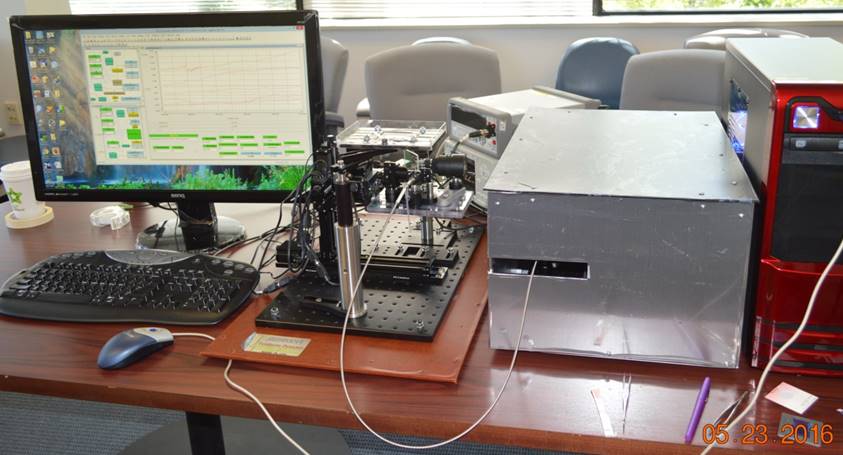
Fiber coupled integrated terahertz spectrometer, nanoscanner and 3D imager
Fiber coupled desktop system
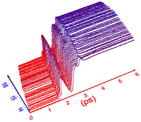
Evolution of terahertz time-domain signal at increasing depth

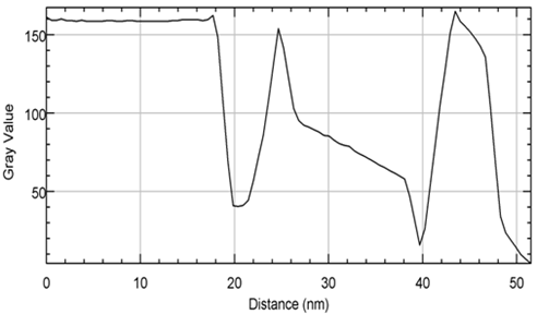
Left: 3D image of epitaxial SiGe layer on top of the Ge lattice structure grown
on Si wafer. Right: Thickness of the top layer is ~18 nm.
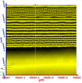
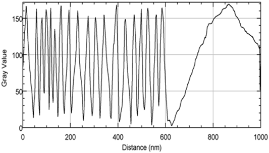
Left: 3D image of epitaxial Ge lattice structure grown on Si wafer. Right:
Thickness of the Ge layer is ~600 nm.