_swellingInteraction.gif)
High resolution terahertz Image Gallery
For more inforation contact:
info@arphotonics.net
Quantum Dots (QDs) Interaction with Polymeric
Ionic Liquid Scaffolds
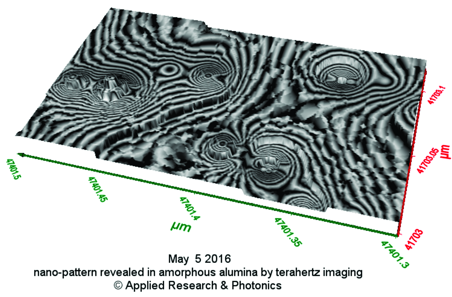
These are real data showing the interaction of QDs with Polymeric Ionic Liquid
as one looks deeper from the surface to inwards (up to 500 nm). Notice the
change in the scaffolding pattern around the QDs.
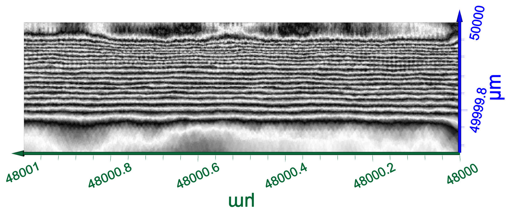
Epitaxial Semiconductor: Different layers identified by difference in
lattice structure
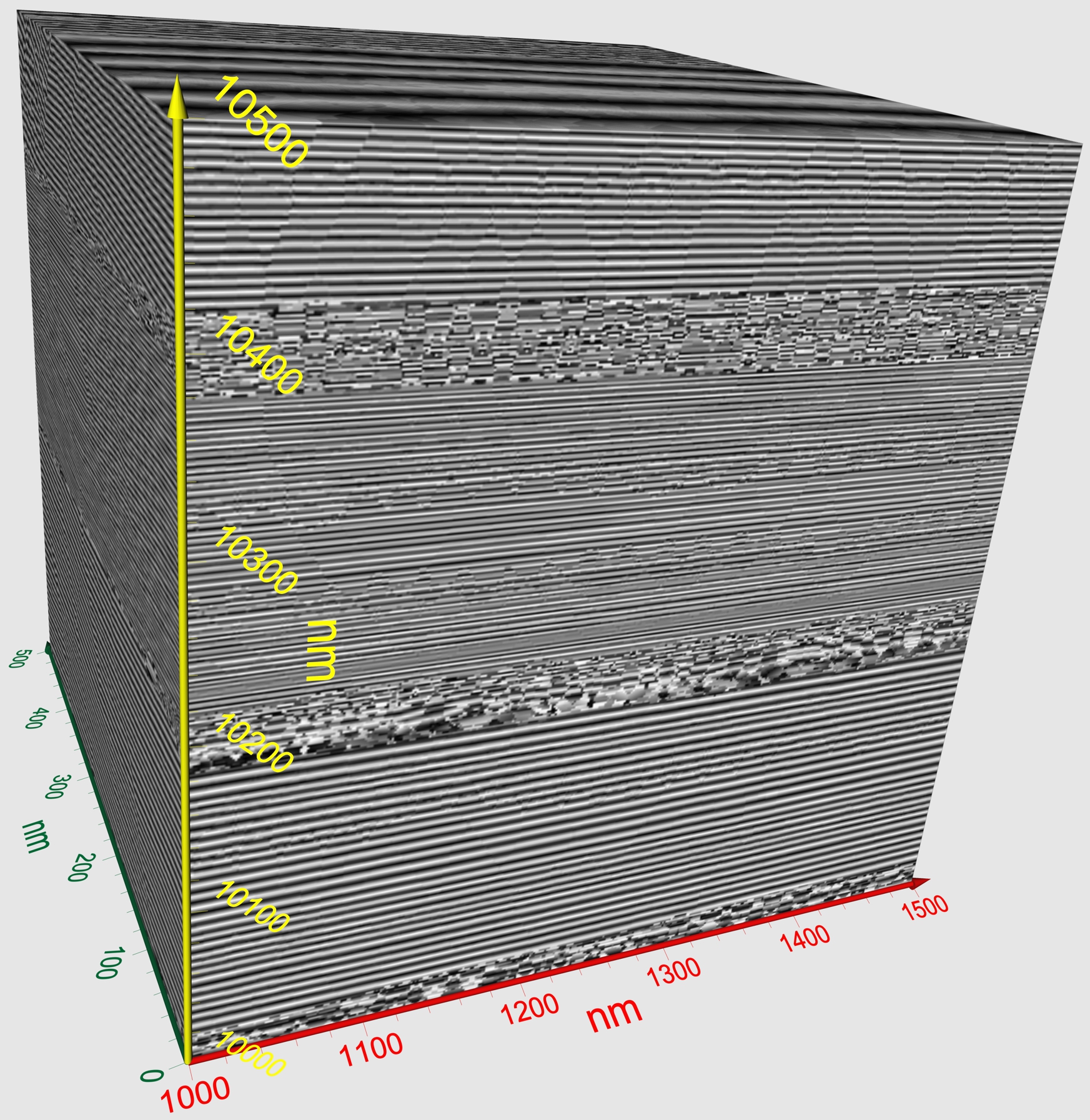
Lattice stacking fault in epitaxially grown semiconductors
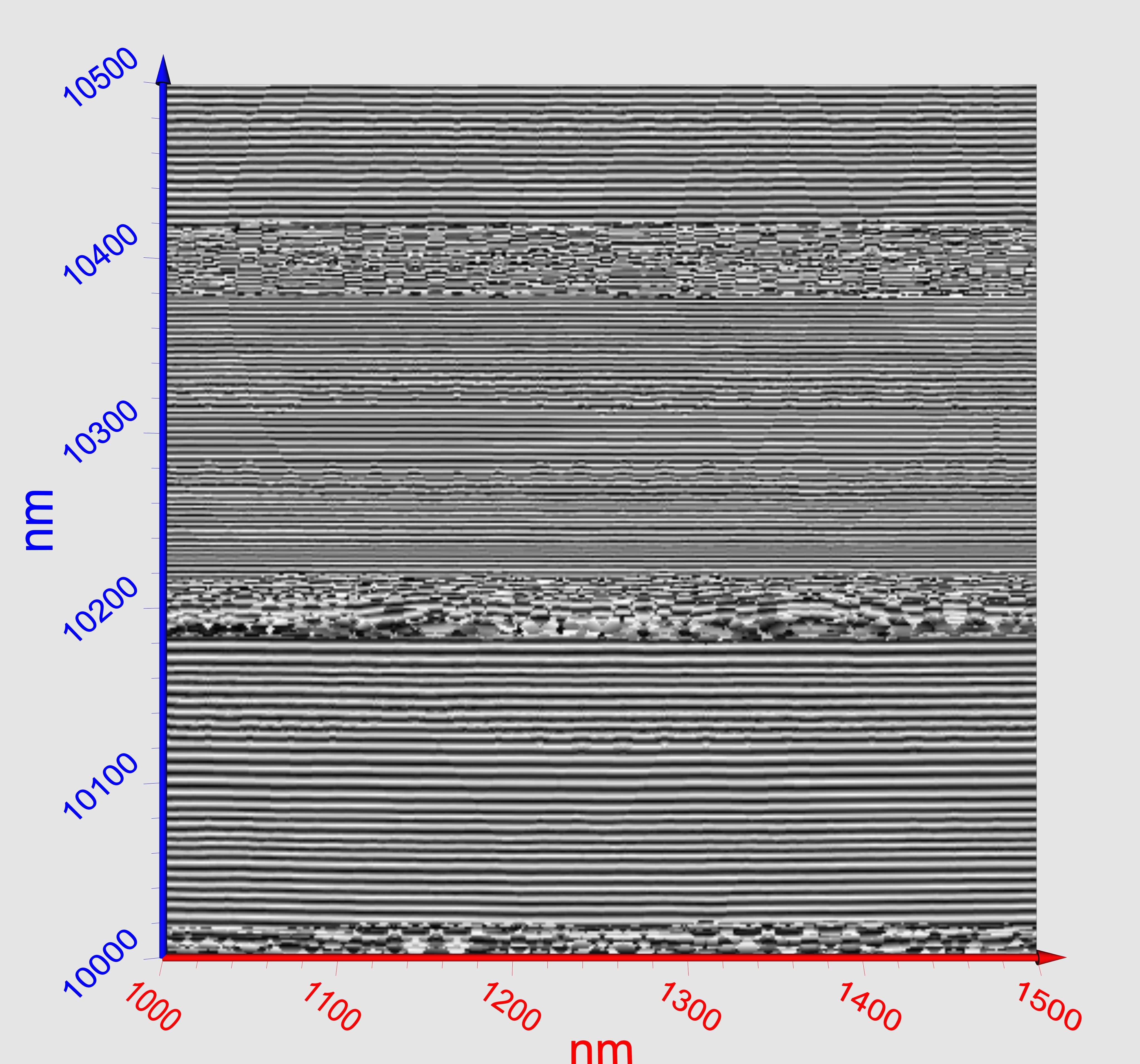
(a) Lattice stacking fault. (b) Planar image showing lattice planes and
boundary. (c) Graphical analysis of dimensions.
Carbon nanotube film on Si wafer: (a) unaligned (b) 60° aligned
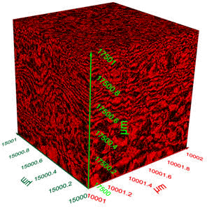
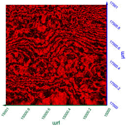
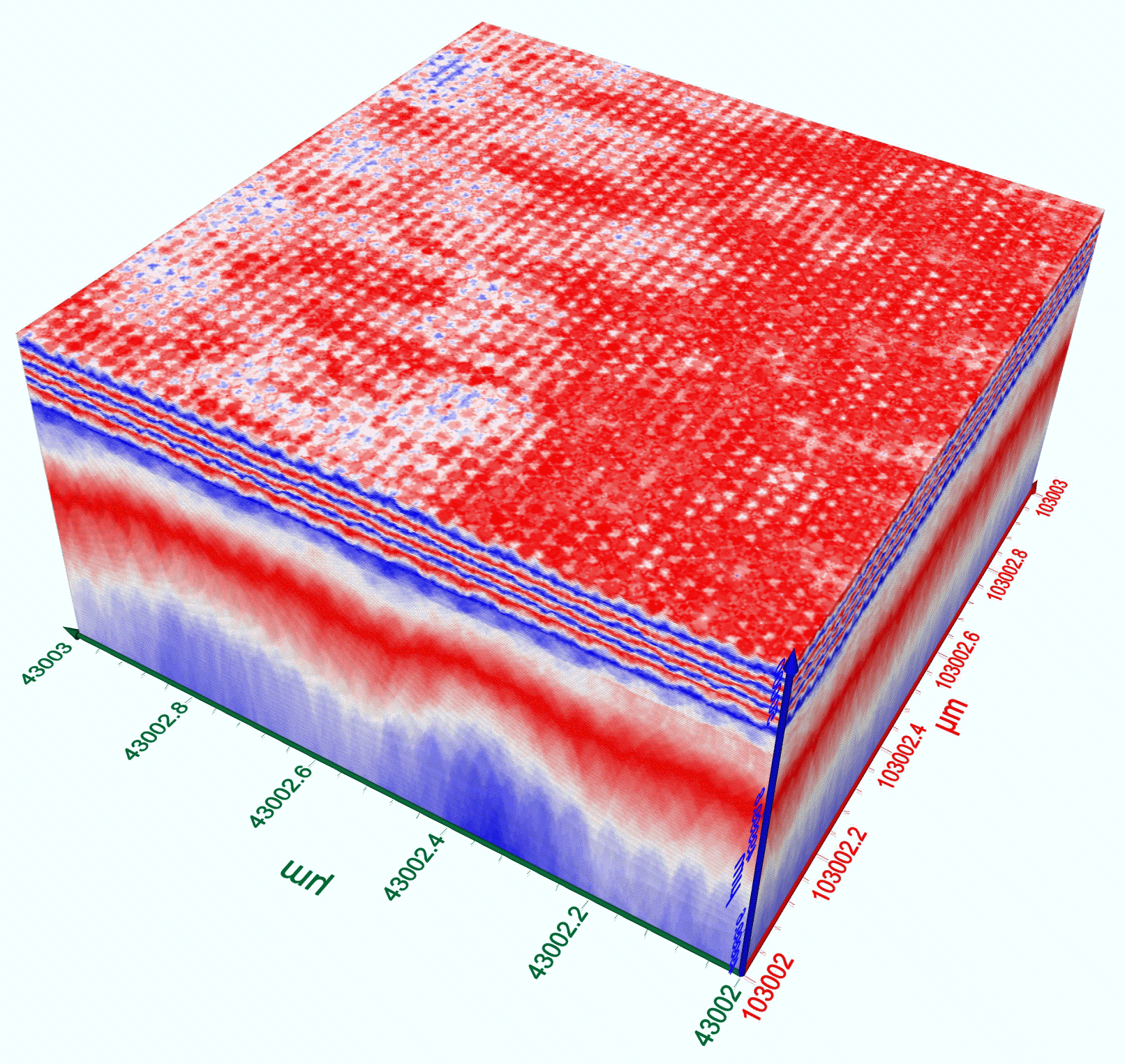
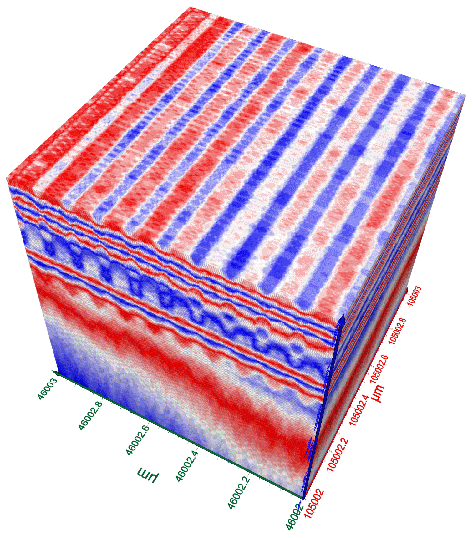
(a) Three dimensional image of 1 cubic micron volume of a “GaN on Si” wafer. (b) One square micron surface image of the same (YZ plane). Distorted lattice patterns are visible indicating damages of the GaN layer.

(a) 3D image of graphene exfoliate layers on Si wafer. (b) A single side (YZ surface) extracted from (a)
![]()
© 2002-2017
Applied Research & Photonics, Inc.
Disclaimer: Any and all information including any specifications on this web may change at anytime at ARP's discretion.